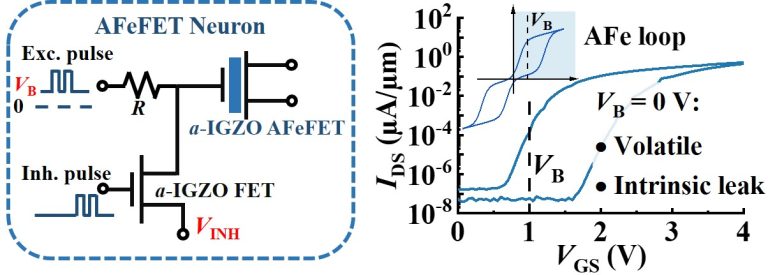
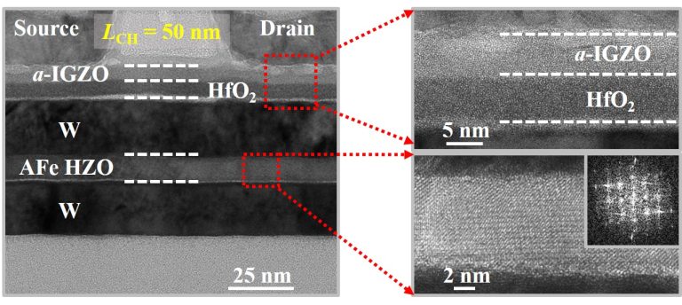
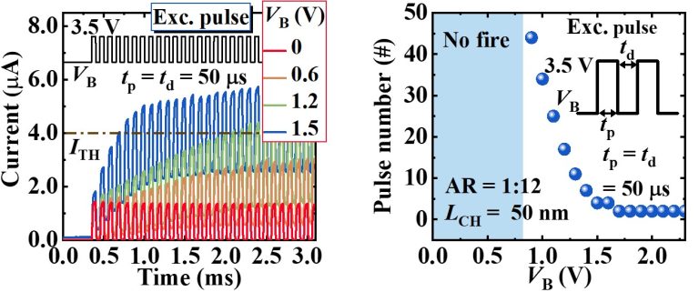
A capacitor-free anti-ferroelectric field-effect transistor (AFeFET)-based neuron with excitatory and inhibitory connections is studied using a metal-oxide a-IGZO channel. The AFeFETs adopt the metal-ferroelectric-metal-insulator-semiconductor (MFMIS) structure to tune the area ratio (AR) between the AFe HZO layer and the metal-oxide-semiconductor (MOS) layer, thus engineering the voltage distribution across the gate stack and optimizing the device characteristics. Due to the unipolar-voltage-drive mode of AFeFETs, a high endurance of more than 109 cycles is achieved. The channel length (LCH) scaling effect is also investigated by scaling the LCH down to 50 nm. Notably, the inherent volatile feature and leaky speed of the a-IGZO AFeFET-based neuron can be balanced by adjusting the base voltage (VB) of the input excitatory pulses, therefore tuning the pulse number for firing. With the integration of a-IGZO FeFET-based synapses, a two-layer SNN is carried out for unsupervised learning using the spike-timing-dependent plasticity (STDP) method, showing a high learning accuracy of 91.4%.
[1] C. Sun, X. Wang, H. Xu, J. Zhang, Z. Zheng, Q. Kong, Y. Kang, K. Han, L. Jiao, Z. Zhou, Y. Chen, D. Zhang, G. Liu, L. Liu, and X. Gong, “Novel a-IGZO anti-ferroelectric FET LIF neuron with co-integrated ferroelectric FET synapse for spiking neural networks,” in 2022 IEEE International Electron Devices Meeting (IEDM), 2022, p. 2.1.1-2.1.4.
[2] C. Sun, X. Wang, H. Xu, J. Zhang, Z. Zheng, Q. Kong, L. Jiao, Y. Chen, and X. Gong, “Anti-ferroelectric FET-based leaky integrate-and-fire neuron with metal-oxide channel towards spiking neural networks,” IEEE Transactions on Electron Devices, to be submitted.

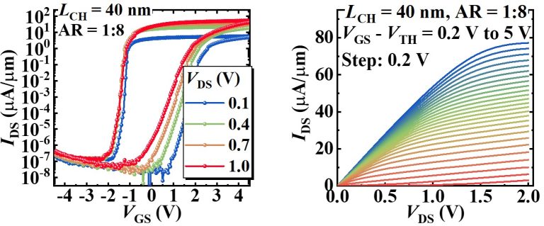
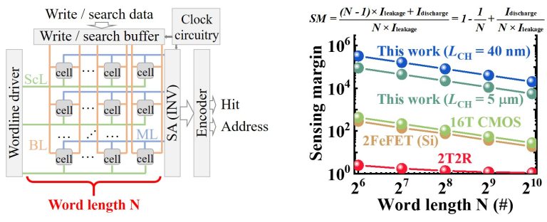
High-performance a-IGZO FeFETs with a metal-ferroelectric-metal-insulator-semiconductor (MFMIS) structure and a fully functional TCAM cell using two a-IGZO FeFETs are realized. The MFMIS structure provides the flexibility of designing the area ratio (AR) between the ferroelectric layer (AFe) and the metal-oxide-semiconductor (MOS) layer (AMOS) to engineer the voltage distribution across the ferroelectric and insulating layers. Here, the AFe is the area of the ferroelectric capacitor, while the AMOS is the overlap between the internal floating gate and the channel. The thermal budget of the device fabrication is within 400 °C with BEOL compatibility. High-performance a-IGZO FeFETs with the normally-off feature, large MW of 2.9 V, good retention of more than 10 years, and decent endurance of 108 cycles are fabricated. Notably, improvement in ON current (ION) and ION/IOFF is realized by scaling the LCH to 40 nm with a slight degradation of the MW from 2.9 to 2.8 V. With the added advantage of large ION/IOFF of the a-IGZO FeFETs, simulations calibrated with the experimental results show that TCAMs using a-IGZO FeFETs have much larger sensing margins over 16T-CMOS, two-transistor-two-ReRAM (2T2R), and Si-based 2FeFET.
[1] C. Sun, K. Han, S. Samanta, Q. Kong, J. Zhang, H. Xu, X. Wang, A. Kumar, C. Wang, Z. Zheng, X. Yin, K. Ni, and X. Gong, “First demonstration of BEOL-compatible ferroelectric TCAM featuring a-IGZO Fe-TFTs with large memory window of 2.9 V, scaled channel length of 40 nm, and high endurance of 108 cycles,” in 2021 Symposium on VLSI Technology, Jun. 2021, pp. 1–2.
[2] C. Sun, K. Han, S. Samanta, Q. Kong, J. Zhang, H. Xu, X. Wang, A. Kumar, C. Wang, Z. Zheng, X. Yin, K. Ni, and X. Gong, “Highly scaled InGaZnO ferroelectric field-effect transistors and ternary content-addressable memory,” IEEE Transactions on Electron Devices, vol. 69, no. 9, pp. 5262–5269, Sep. 2022.
See More: Device Modeling of a-IGZO FeFETs with Various ARs

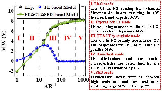
Comprehensive experiments and modeling are performed to understand the influence of ferroelectric (FE) polarization switching, charge trapping (CT) in the floating gate (FG) from both the control gate (CG) and channel, and soft breakdown (SBD) on the characteristics of the FeFETs having a metal-ferroelectric-metal-insulator-semiconductor (MFMIS) structure. Assisted by extensive experiments and guided by rigorous understanding through experiment-simulation interaction, key findings are summarized: (1) SBD could happen as AR (AFe/AMOS) reduces to a certain value through analysis of the devices with AR from 0.001 to 1; (2) previous FE-only based model without considering CT in FG and SBD fails to explain various trends in a wide range of AR. (3) The recently discovered phenomenon of MW being higher than 2VC (the limitation of FeFETs, VC is the coercive voltage of the ferroelectric layer) can be explained by the combined effect of CT in FG and SBD. These findings motivated us to develop a comprehensive and accurate FE&CT&SBD-based model which incorporates the impact of FE, CT in FG, and SBD. The excellent agreement between our model and the experimental data allows us to propose, for the first time, five operation modes of the MFMIS structure, providing the guidelines for device optimization and application.
[1] X. Wang*, C. Sun*, Z. Zheng, L. Jiao, Z. Zhou, D. Zhang, G. Liu, Q. Kong, J. Zhang, H. Xu, K. Han, Y. Kang, L. Liu, and X. Gong, “Deep insights into the interplay of polarization switching, charge trapping, and soft breakdown in metal-ferroelectric-metal-insulator-semiconductor structure: Experiment and modeling,” in 2022 IEEE International Electron Devices Meeting (IEDM), 2022, p. 13.3.1-13.3.4. (Co-first author)
[2] X. Wang*, C. Sun*, Z. Zheng, L. Jiao, Z. Zhou, D. Zhang, G. Liu, and X. Gong, “Comprehensive experiments and modeling applicable for ferroelectric transistors with an MFMIS structure and a wide range of area ratios: Unveiling the operation mechanisms,” IEEE Transactions on Electron Devices, to be submitted. (Co-first author)

By cooperating the amorphous indium-gallium-zinc-oxide (a-IGZO) channel with the ferroelectric HfZrO2 (HZO), a-IGZO FeFETs with MFS and MFMIS structures are investigated. Due to the voltage division and channel depletion issues, the FeFETs with an MFS structure show a non-erasable threshold voltage (VTH) state. These issues can be settled by adopting an FG to form the MFMIS device structure, providing the flexibility to tune the voltage distribution by adjusting the area ratio (AR) and achieving a large MW of ~3.1 V at room temperature. A high ION/IOFF ratio of more than 7 orders is also realized when the VDS is 1.3 V. In addition, the temperature-dependent operation of a-IGZO FeFETs from -40 to 100 °C reveals that the MW increases with increasing temperature due to the enhancement of remanent polarization (Pr) without the degradation of current and ION/IOFF ratio. Thus, VTH stability could be improved by engineering the electron tunneling in the MFMIS structure to compensate for the negative VTH shift due to higher Ncarrier in a-IGZO at higher temperatures.

[1] (Thesis, Chapter 3) C. Sun, “Amorphous Indium-Gallium-Zinc-Oxide-Based Transistors for Emerging Non-Volatile Memory and Neuromorphic Computing Applications,” National University of Singapore, 2023.
[2] C. Sun, Z. Zheng, K. Han, S. Samanta, J. Zhou, Q. Kong, J. Zhang, H. Xu, A. Kumar, C. Wang, and X. Gong, “Temperature-dependent operation of InGaZnO ferroelectric thin-film transistors with a metal-ferroelectric-metal-insulator-semiconductor structure,” IEEE Electron Device Letters, vol. 42, no. 12, pp. 1786–1789, Dec. 2021.
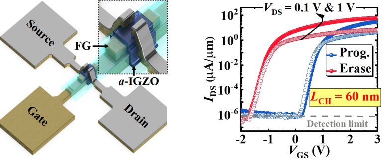
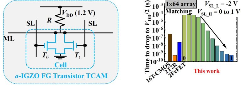
Amorphous indium-gallium-zinc-oxide (a-IGZO) floating-gate (FG) transistors with outstanding electrical characteristics, including low IOFF of less than 10-7 µA/µm, large ION/IOFF of 1×10⁸, low subthreshold swing (SS) of ~80 mV per decade, and high mobility of 32.6 cm2/V∙s are realized in this work. The a-IGZO FG transistors show a large memory window (MW) of 1.8 V at a low operating voltage with more than 10 years of retention. The endurance measurement of 1000 cycles slightly reduces the MW from 1.8 to 1.6 V. Moreover, the transistors still offer an MW of 1.4 V even at a high temperature of 80 °C. By scaling the LCH to 60 nm, a record-high ON current (ION) of 127 µA/µm is obtained, which is much higher than reported flash transistors using an a-IGZO channel while maintaining the MW larger than 1.5 V. Furthermore, an area-efficient ternary content-addressable memory (TCAM) cell with only two parallel-connected a-IGZO FG transistors is demonstrated under a low process temperature of 300 °C. Functionalities of writing and searching are realized. Using experimentally calibrated models, array-level simulations to benchmark the scalability, search energy, and search delay of TCAM arrays are further performed. The results highlight that, compared with 16T-CMOS, two-transistor-two-ReRAM (2T2R), and Si 2FeFET TCAMs, the TCAM array using a-IGZO FG transistors exhibits at least a 240× improvement in array-size scalability and a 2.7-fold reduction in search energy.
[1] C. Sun, C. Li, S. Samanta, K. Han, Z. Zheng, J. Zhang, Q. Kong, H. Xu, Z. Zhou, Y. Chen, C. Zhuo, K. Ni, X. Yin, and X. Gong, “Computational associative memory with amorphous metal-oxide channel 3D NAND-compatible floating-gate transistors,” Advanced Electronic Materials, vol. 8, no. 12, p. 2200643, 2022

This work presents a power-efficient, scalable, and robust approach to the design of an eDRAM-based compute-in-memory (CiM) accelerator for artificial neural networks using the back-end-of-line (BEOL) compatible amorphous-indium-gallium-zinc oxide (a-IGZO) TFT technology. The highlights include: (i) IGZO TFTs with ultra-low leakage current, high on-state current of 157μA/μm for 45nm devices, and excellent subthreshold swing as low as 71mV/dec and 105mV/dec for 5μm and 45nm devices, respectively; (ii) a novel 4T1C eDRAM differential CiM cell that tolerates σ(VTH)=50mV and σ(CC)/CC=2% for accurate 128-row 8-bit MAC operations, and achieves >50× longer retention time during computing than the prior TFT eDRAM cells; (iii) a charge-domain coupling-based CiM technique that enables low sensing complexity and high computing power efficiency by avoiding DC power and complex timing control. Experiment-calibrated benchmarking in VGG-8 network for CIFAR-10 image classification tasks shows 2092 TOPS/W power efficiency for the CiM core and 795 TOPS/W including peripherals, and outperforms prior TFT and CMOS-based CiM approaches in a range of event density.
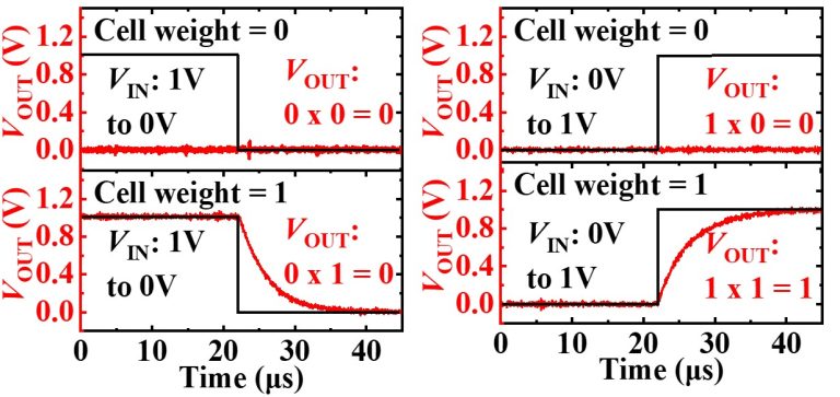
[1] J. Liu*, C. Sun*, W. Tang, Z. Zheng, Y. Liu, H. Yang, C. Jiang, K. Ni, X. Gong, and X. Li, “Low-power and scalable retention-enhanced IGZO TFT eDRAM-based charge-domain computing,” in 2021 IEEE International Electron Devices Meeting (IEDM), Dec. 2021, p. 21.1.1-21.1.4. (Co-first author)
Part I: Relaxation of tensile strain by ion implantation

The relaxation of tensile strain in fully-depleted (FD) strained silicon-on-insulator (SSOI) by means of ion implantation is experimentally demonstrated. This could enable SiGe p-channel field-effect transistors (pFETs) with high compressive strain (after ion implantation and Ge condensation) to be formed together with Si n-channel field-effect transistors (nFETs) with high tensile strain on the same substrate. From simulations in advanced technology node, 0.8% strain of nFETs and -0.9% strain of pFETs in fin structures can provide saturation drain current and peak transconductance (Gm) enhancements of ~20-30%. fT and fmax benefit greatly from strain across the entire range of VG, with their peak values increasing significantly, thus allowing SSOI devices to meet 5G targets. In addition, forward back-bias shifts fT and fmax curves towards lower |VG|, enabling reduced power consumption at the same high performance and providing better linearity. Hence, the ability to form highly strained nFETs and pFETs together on a common fully depleted SSOI (FD-SSOI) substrate paves the way for it to become the ultimate high-performance complementary metal-oxide-semiconductor (CMOS) platform for 5G RF and logic circuits.
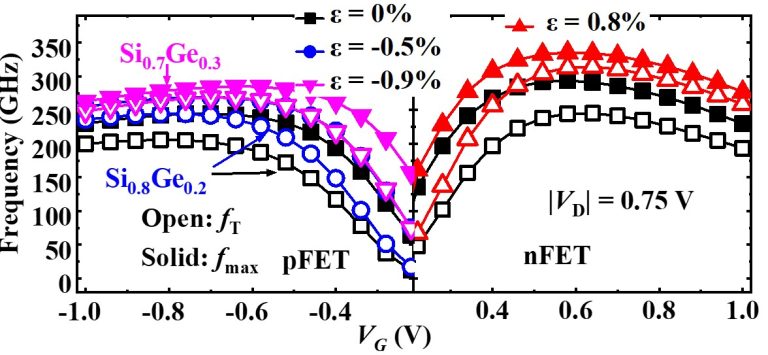
[1] C. Sun, J. Liang, H. Xu, E. Kong, B.-Y. Nguyen, A. Vandooren, W. Schwarzenbach, C. Maleville, V. Barral, R. Berthelon, O. Weber, F. Arnaud, A. V. Y. Thean, and X. Gong, “Enabling UTBB strained SOI platform for co-integration of logic and RF: Implant-induced strain relaxation and comb-like device architecture,” in 2020 IEEE Symposium on VLSI Technology, Jun. 2020, pp. 1–2.
[2] C. Sun, H. Xu, J. Liang, E. Y.-J. Kong, B.-Y. Nguyen, W. Schwarzenbach, C. Maleville, R. Berthelon, O. Weber, F. Arnaud, X. Wang, A. V.-Y. Thean, and X. Gong, “Strained silicon-on-insulator platform for co-integration of logic and RF—Part I: Implant-induced strain relaxation,” IEEE Transactions on Electron Devices, vol. 68, no. 4, pp. 1425–1431, Apr. 2021.
Part II: Novel Comb-like device structure
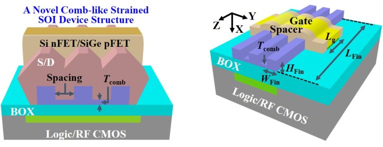
Based on an SSOI platform which could enable the co-integration of highly tensile-strained Si n-channel field-effect-transistors (nFETs) and compressive-strained SiGe p-channel FETs (pFETs) on the same substrate for both logic and 5G RF circuits, a Comb-like device structure is proposed within the strained SOI platform for further improvement in the electrostatic, DC, and RF performances over the unstrained SOI FinFETs counterpart. It is demonstrated that the peak Gm of strained Comb-like Si nFETs can be improved by 35% over unstrained n-type FinFETs SOI. The improvements of fT by 22% and fmax by 36% over no-comb devices are also observed. Furthermore, the linearity of fT and fmax has been greatly improved by introducing forward body biasing on the Comb-like device structure.
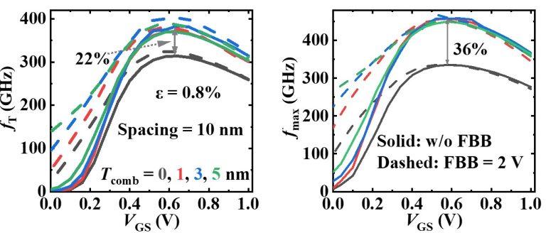
[1] C. Sun, J. Liang, H. Xu, E. Kong, B.-Y. Nguyen, A. Vandooren, W. Schwarzenbach, C. Maleville, V. Barral, R. Berthelon, O. Weber, F. Arnaud, A. V. Y. Thean, and X. Gong, “Enabling UTBB strained SOI platform for co-integration of logic and RF: Implant-induced strain relaxation and comb-like device architecture,” in 2020 IEEE Symposium on VLSI Technology, Jun. 2020, pp. 1–2.
[2] J. Liang*, C. Sun*, H. Xu, E. Y.-J. Kong, B.-Y. Nguyen, W. Schwarzenbach, C. Maleville, R. Berthelon, O. Weber, F. Arnaud, A. V.-Y. Thean, and X. Gong, “Strained silicon-on-insulator platform for co-integration of logic and RF—Part II: Comb-like device architecture,” IEEE Transactions on Electron Devices, vol. 69, no. 4, pp. 1769–1775, Apr. 2022. (Co-first author)
